Johnny One Note Flippers.com Left Flipper   Right Flipper   OnLine Shopping Cart Click here to order Parts  Tweeting games just in!    Instagram

index sitemap advanced
site search by freefind


Game Plan Pinball tech tips page... last modified December 23, 2022

Modified RESET - much simpler! (80272 bytes) On another note, I have designed a replacement for the RESET circuit that often fails in these games-much simpler as you replace a bunch of resistors and transistors with a single IC (called a CPU Supervisor), and cut and jumper a few traces. I shall expand that here in the future.
GP-MPU2-2764.jpg (270691 bytes) To replace the ROM memory with a single EPROM (2764) all you need to do is first program the 2764 with the game code loading from 0000h up. Next bend out pins #20, 22, and 23 on the 2764. Then solder a jumper wire on pins #26, 27, 28 and 1 (tie all to 5VDC). Now refer to the photo to the left and add jumper wires from 2764-P2 to A12, 2764-P23 to A11, 2764-P22 to A15, and 2764-P20 to /MREQ. Works for me! 
GamePlan-Corrosion.jpg (165309 bytes) Battery corrosion is a real problem for Game Plan MPUs, please read up the details on my battery page...
GamePlanMPU-bad-cap.jpg (71464 bytes) Weird Solenoid or Lamp problems? Do you not get any sounds or are they mixed up, yet the MPU and Sound boards both seem to be ok? Then take a look at this capacitor - it might be broken or leaky. This capacitor is a critical timing capacitor. While you are in there if you have any switch matrix trouble then replace the 0.1 (104) capacitor just below and to the left of this.

Replacing the original Harris HM6551-9 CMOS RAMs with a pair of 5101s
(best to wait until I rewrite this section in early 2022 - unless you can understand what I am trying to do here - one thing to watch for is that you have fast 5101s)

GP-MPU2-CutPin19_18-1.jpg (125140 bytes) MPU-2 (and MPU-1) 1st cut solder pads between Pins 18 & 19 on both U6 and U7 - Note for MPU1 we now have a replacement NVRAM module to replace the 6551s and remove the battery permanently. - but it doesn't fit MPU-2(yet)
GP-MPU2-CutPin19_18-2.jpg (147612 bytes) MPU-2 (and MPU-1) should look like this now. 
GP-MPU2-CutU5Pin8.jpg (100449 bytes) MPU-2 (and MPU-1) cut trace from U5-Pin 8
GP-MPU1-PiggyBack74LS04.jpg (94582 bytes) MPU-1 mods to topside of MPU - add 74(LS/HCT)04 (Piggy Back) on top of U5 (print out image). You need this inverter as there are no free gates left on the MPU-1 PCB, and we will need two inverter gates. For the MPU-1 PCB you have to connect Pin 9 of the Piggy Back to U5-Pin 8, bend out Piggy Back-Pin 8 and add a jumper to the cut trace. 

This is almost identical to the MPU-2 mods except that MPU-2 has  a spare inverter gate on U24 that we will use to invert U6/7-Pin17, thus we will only need one gate on the Piggy Back.

Found a way to get rid of the Piggyback 74LS04. Simply run a jumper from U6 pin 18 (5101 OE) to U11 pin 21 (CPU /RD pin) - more to come when I have some time...

GP-MPU1-CutU5-P8.jpg (75366 bytes) MPU-1 alternate picture showing cut trace at U5-Pin8 and jumper to Piggy Back-Pin 8 and jumpers to U6-pins 20 and 18 as described below.
GP-MPU1-ModToPin18-2.jpg (177108 bytes) MPU-1 mods to underside of MPU board (same solder pad cuts as MPU-2 below)
GP-MPU2-ModsMarked.jpg (188232 bytes) MPU-2 Now...(print out this image)...add jumpers between U6-Pin 20 and Piggy Back-Pin 11 (input), then jumper between U6-Pin 18 and Piggy Back-Pin 10 (output). This sets up the OE pin so it is the opposite of R/W. Add jumper between U6-Pin 19 and U7-Pin 19 (note that U6 & U7 Pin 18's are already connected with a trace on the top side of the PCB). Next jumper U5-Pin 8 to U24-Pin 11, then jumper U24-Pin 10 to U6-Pin 17.
GP-MPU2-PiggyBack74X04-Comments.jpg (144910 bytes) MPU-2 Location of Piggy Back and the required connections.


Troubleshooting:

> Flashes 4 times then stops. I have changed U17 and U4 as the repair guide states. I have tested continuity from all pins, I also went backward to U5 and changed that. Still, only 4 flashes. Any suggestions are appreciated.

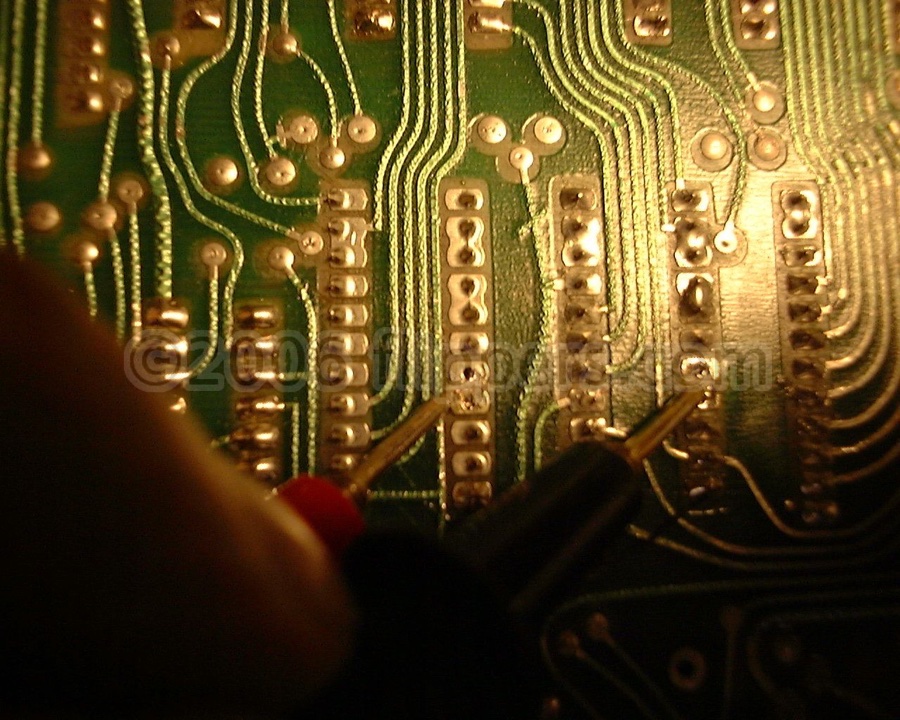
You need a Logic Probe or Oscilloscope at this point.

Check inputs to U14 - pins 20 through 23 - they should all be pulsing.

If good then check U14 outputs pins 14 - 17 inclusive, again they should be pulsing.

If bad, check U17 pins 37 through 40 inclusive, are they all pulsing? If yes, then there is a connection problem between U17 and U14 pins. If no, then do a continuity check to ground or Vcc on those four pins - any shorted to ground or Vcc?

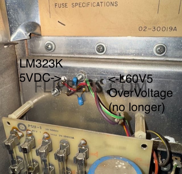
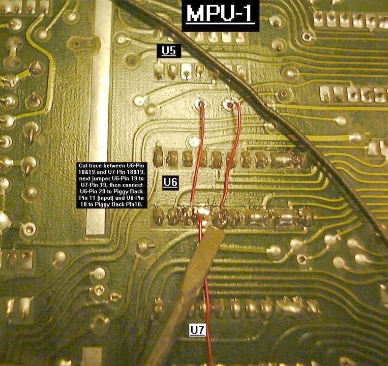
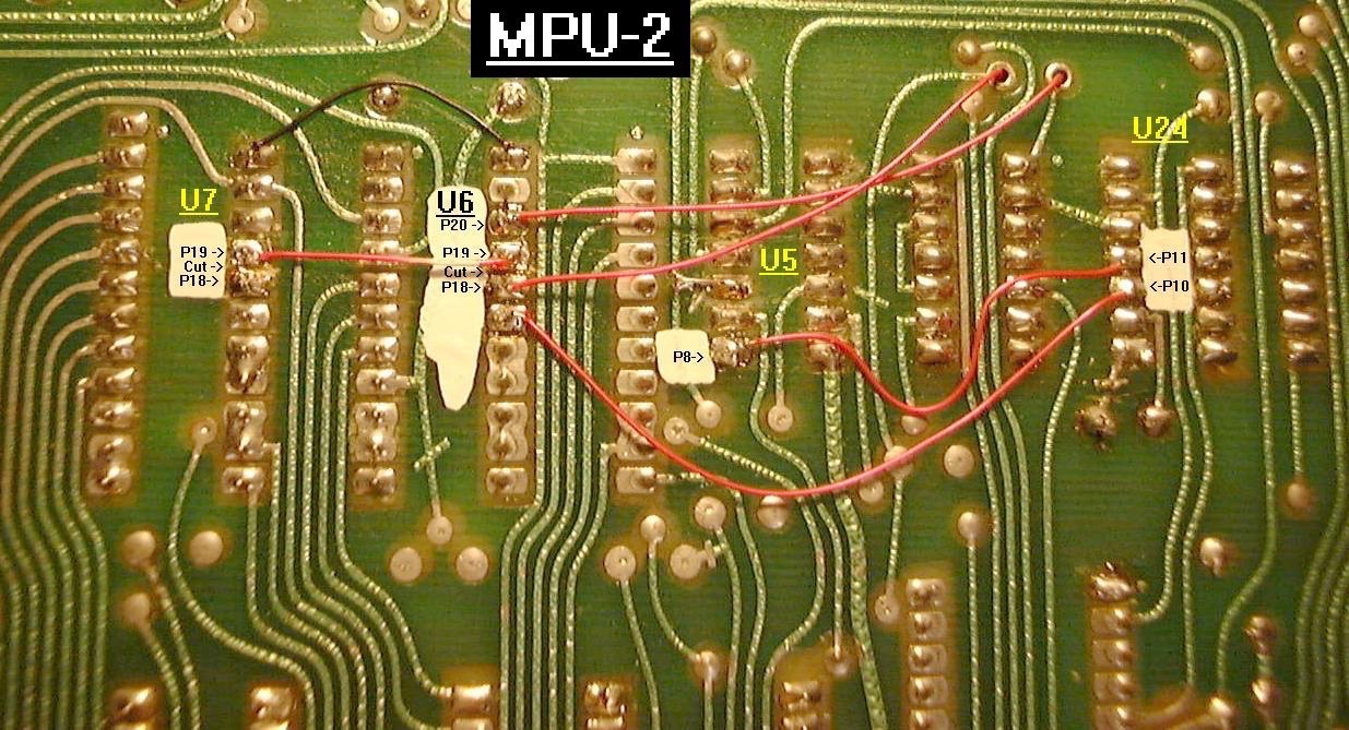
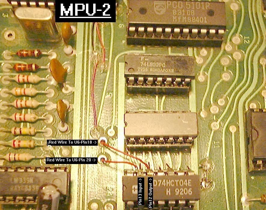
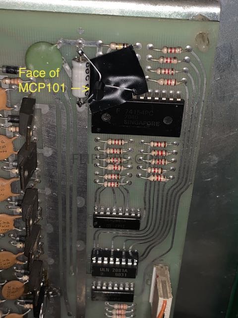
Game Plan THUNK! - When some GP machines are started they sometimes fire one or more solenoids such as the ball kicker, drop target, etc. This can be annoying as well as potentially hazardous to the driver transistor so we have fixed this by adding a Reset Supervisor IC MCP-101 to pin 19 of the 74154 1-of-16 decoder IC. Cut pin 19 very close to the solder pad and bend it up, then solder the MCP-101 to the filter capacitor and Pin 19 as shown here...

Reset IC MCP101


You can order a replacement MPU (around $195US) for either cocktail or regular Game Plan games from:

(Summer, 2022) Jim Francesangeli is no longer making replacement MPUs, however there is a new source. Coming shortly...

Tips for specific games (from rec.games.pinball newsgroup):

SUPER NOVA:
Problems with the SWITCH CATCHER (PCB under playfield near left flipper):

>>
>>> When I disconnect the Switch Catcher from the game (Supernova)
>>> everything works. When I attach it the game will not start. I have
>>> replaced the three major IC's and checked all caps, diodes, and
>>> resistors.
>>> Anyone have any thoughts?
>> Yes this can easily be fixed, If everything works fine when the switch
>> catcher is disconnected then this will fix it...
>
> The "switch catcher" Seems to control All of the switches that stem
> from the spinwheel at the top of the PF. It is located at the bottom
> left under the PF and has a 15 pin connector. There are the 4
> switches, 4 strobes, and 4 lines. It also gets 2 ground feeds and 1
> +5v power feed. With the switch catcher disconnected, the above 4
> switches do NOT work so leaving it off is really a bum option.

Switch Catcher - #02-70051B.

It looks like this circuit board is indeed designed to "catch" switches with short duration impulses using flip-flop logic that is tripped when a switch is closed and is reset when the next strobe pulse comes along.

I checked the PCB on my working Super Nova and found the following pins (counting from the front of the cabinet to the back) are all High (roughly 5.0VDC) #1, 2, 3, 4 (could be pulsing), 5, 6 (Vcc) 8 (High pulsing low), and 9 (could be pulsing).

Switch inputs are #1, 2, 3, and 5 - all should be High as the switches should be open.

The common./ground pin is (of course) Low - #13 & #12 (no wire to 12).

Pulsing pins are the Strobe Inputs - #7 (ST-0), #10 (ST-1), #14 (ST-2) and #15 (ST-3).

If any of your reading are different, then first check the PCB for cracked/cold solder connections to the long Molex pin row, then check switches for jammed closed, finally do the Diode Test on the TTL and LM339 gates...

http://www.flippers.com/service.html#tips (diode test)

John :-#)#


(jrr-at-flippers-dot-com for those who do not have their browser set to open their email client)
Click here (spam@fl... is valid) to send us email->email.gif (11071 bytes)    creditcards.gif (9926 bytes)
Hablo espanol? Si! Email Alexander...
All information on this site is Copyright (©) 1997 through 2024 by John's Jukes Ltd.
MOVED (as of May, 2017) to 7 - 3979 Marine Way, Burnaby, BC, Canada V5J 5E3
(604)872-5757